

The power electronics industry is responsible for products used by billions of people: smartphones, televisions, certain car parts, and even components in motors and household objects. With such a diverse array of applications, many design requirements are considered during the making of these products, including power and energy density, cost, and customer safety. Arkansas Power Electronics International (APEI), a USA-based company, is refining designs for power packaging to control thermal management in power electronics devices, increase efficiency, and lower cost.
Designing Power Electronics for Optimal Thermal Management
Many factors influence the performance of power electronics devices. For example, ideal operating conditions may require a specific temperature range, voltage level, and switching frequency that, if unmaintained, can cause problems such as failure, increased resistance, reduced efficiency, or voltage spikes.
This is why a team at APEI decided to develop a new power module — a package meant to contain power components, cool electronics devices, and connect them to other circuits — with improved thermal management capabilities and performance. Brice McPherson, lead engineer, says that their goal was to create a power package flexible enough to be used for many applications. It needed to be small, easy to configure, and exhibit low inductance with good thermal conductivity.
The figure below shows their new design, which is only a little larger than a U.S. quarter:
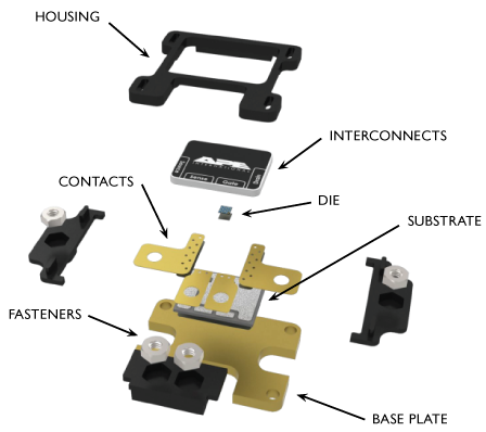

The power package, showing individual components (left) and the entire assembly (right).
Cooling Off the Heat: Harsh Environments Demand Stable Materials
The team began with two materials for comparison: gallium nitride (GaN) and silicon carbide (SiC). The advantage of these materials is that both are wide-bandgap semiconductors that can be safely used at high frequencies and temperatures. This means that they can withstand harsh environments where most electronics have a tendency to fail. For instance, it’s something of a challenge to protect electronics used in drilling equipment, where pressure and temperature increase dramatically very quickly, or create electronics that can survive being sent to the surface of Venus.
McPherson used COMSOL software to aid their design process, analyzing the thermal and electrical response of the new power package when it included each of the chosen materials. He analyzed thermal conduction (aiming to maximize it and reduce thermal resistance), inductance, and device size.
“Designing for low thermal resistance involves selecting materials with high thermal conductivity, reducing the distance heat travels to leave the layers, and optimizing layer thickness to take advantage of thermal spreading,” he explained. “That’s where parametric modeling is your best friend: you can set up parametric sweeps to find out exactly what’s influencing the system the most and get the best compromise among performance, complexity, and cost.”
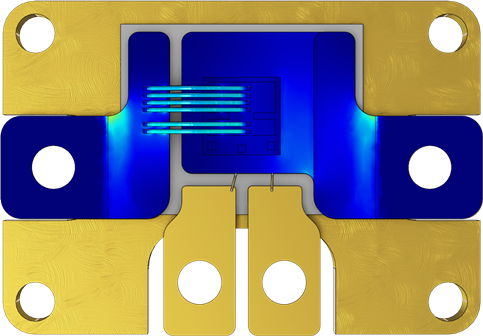
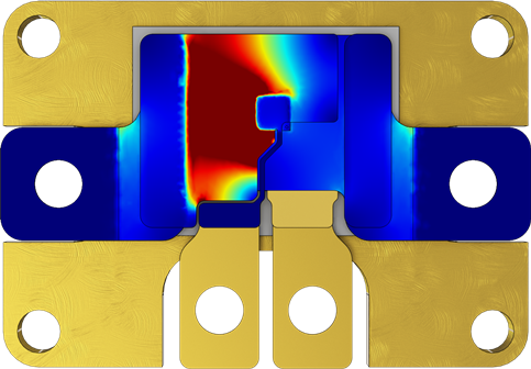
Simulation results overlaid on geometry, showing current density in the SiC package (left) and the GaN package (right). The SiC package displays low density (ideal for higher currents), with the highest concentrations in the wire bonds. The GaN shows a higher density, but has more available area for conduction, which is preferred for low inductance.
McPherson compared his designs to a commonly-used transistor outline package, the TO-254, aiming to improve upon current industry standards. His hope was that APEI’s new design would be able to withstand very high temperatures — above 225°C. The simulation results showed that both the APEI power modules reflected a lower thermal resistance and significantly lower inductance than the TO. The results also indicated that they operated successfully in the specified temperature range.
Providing New Inductance and Thermal Management Capabilities
The team at APEI discovered that optimizing the size of the device and thickness of the base plate were the most influential factors in reducing the inductance of each package. He maximized the cross-sectional area and minimized the current path in an effort to minimize inductance and maximize heat dissipation. The COMSOL Multiphysics results showed that the GaN module exhibited the lowest inductance (7.5 nanohenries). The SiC turned out to be the best choice for cases where high currents and thermal loading were present, processing large amounts of energy in an extremely small area.
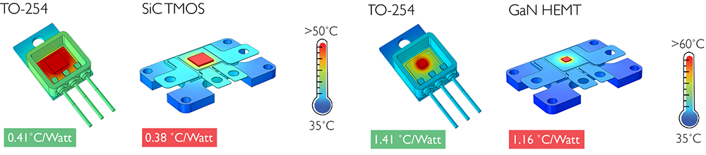
A comparison of thermal resistance among the TO-254, SiC, and GaN power modules based on COMSOL Multiphysics results.
The Results at APEI
The result? Two unique and powerful package options that are flexible enough to address multiple customer needs; operate smoothly with clean, rapid switching; and can withstand the high temperatures and frequencies demanded by extreme applications.
APEI’s new modules have far surpassed the current industry transistors, and are paving the road to new capabilities and unforeseen applications in the power electronics field.


Comments (0)