

It’s possible to measure the far-field response of any scatterer or antenna with the Far-Field Domain feature of the RF Module, an add-on product to the COMSOL Multiphysics® software. For taking it a step further, COMSOL Multiphysics can replicate experimental setups to a greater extent, e.g., antenna gain measurement or emission or immunity testing of a circuit board for addressing EMI/EMC issues, thanks to the finite element method–boundary element method (FEM–BEM) coupling. This coupling can also be used to find wave propagation in the surrounding infinite free space in microstrip patch antenna models. In this blog post, we’ll take a deep dive into modeling transmitter and receiver antennas for line-of-sight (LoS) communication, one of the applications of FEM–BEM coupling.
Line-of-Sight Communication
To understand LoS communication, it’s important to know how the power is received by the antenna. This is given by the well-known Friis transmission formula (in dB) as follows:
Here, \text {P}_\text{t} is transmitted power; \text{P}_\text{r} is received power; \text{G}_\text{t} (\theta_t, \phi_\text{t}) and \text {G}_\text{r} (\theta_\text{r}, \phi_\text{r}) are the gain of the transmitted and received antenna, respectively; and \text {Path Loss} (in dB) is given by
{\lambda} is the operating wavelength and d is the distance between the antennas. This distance typically represents the shortest distance between the antennas in the Fresnel zone. (This zone is an elliptical region formed between the antennas and does not contain any physical obstruction that may interfere with the signal traveling.)

Figure 1. Depiction of the typical LoS communication link.
Now, let’s rearrange Eq. 1 so that, with simulation, we can compare the right-hand side of the new equation (Eq. 3) with an S-parameter obtained from simulation. This equation is as follows:
Here, the left-hand side represents S21 (in dB).
Modeling Transmitter and Receiver Antennas
From the Friis formula, it’s well understood that \text {P}_\text{r} can be maximized by minimizing the path loss. The path loss increases as operating frequencies and/or the distance between transmitter and receiver antenna increases. Figure 2 demonstrates this, with the transmitter and receiver modeled in the FEM domain and coupled with a predefined FEM–BEM coupling. Note that the transmitter is a microstrip patch antenna, with the Lumped Port 1 voltage excitation on in the Electromagnetic Waves, Frequency Domain 3: Tx and Rx Antennas (emw3) interface (also known as the emw3 interface). The receiver is a Yagi–Uda antenna, with the Lumped Port 2 excitation off in the emw3 interface.

Figure 2. The emw3 and embe interfaces are coupled with the Electric Field Coupling multiphysics interface.
You can also visualize the wave propagation from the transmitter to the receiver with the help of the Animation feature (shown below).
The propagation of EM waves from the transmitter to the receiver. This simulation uses the FEM–BEM coupling feature.
In the Friis formula, far-field antenna gain for both antennas is required. These are computed using the Far-Field Domain node in the:
- Electromagnetic Waves, Frequency Domain: For Yagi–Uda Antenna (Rx) (emw) interface — emw interface for short
- Electromagnetic Waves, Frequency Domain 2: For Microstrip Patch Antenna (Tx) (emw2) interface — emw2 interface for short
You can see such interfaces in the image below.
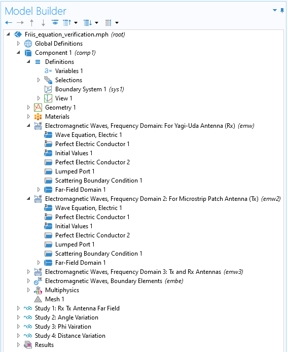
Figure 3. The emw and emw2 interfaces are used to find far-field gains of the Yagi–Uda and microstrip patch antennas.
For comparison, variables are created to formulate the Friis formula (Figure 4). The separation between the antennas is increased, and the received power in terms of the S-parameter is measured (Figure 5).
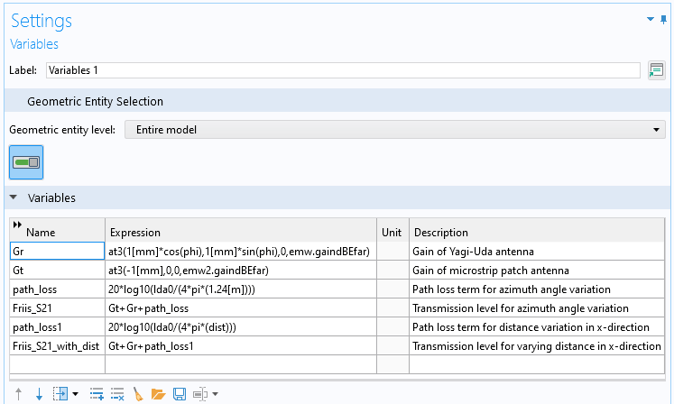
Figure 4. The far-field expressions are used to formulate the Friis equation. Here, lda0 and dist represent the operating free space wavelength and the distance between the Rx and Tx antennas, respectively. To access far-field gain at a particular coordinate defined via the phi angle parameter, a predefined at3() function is used.
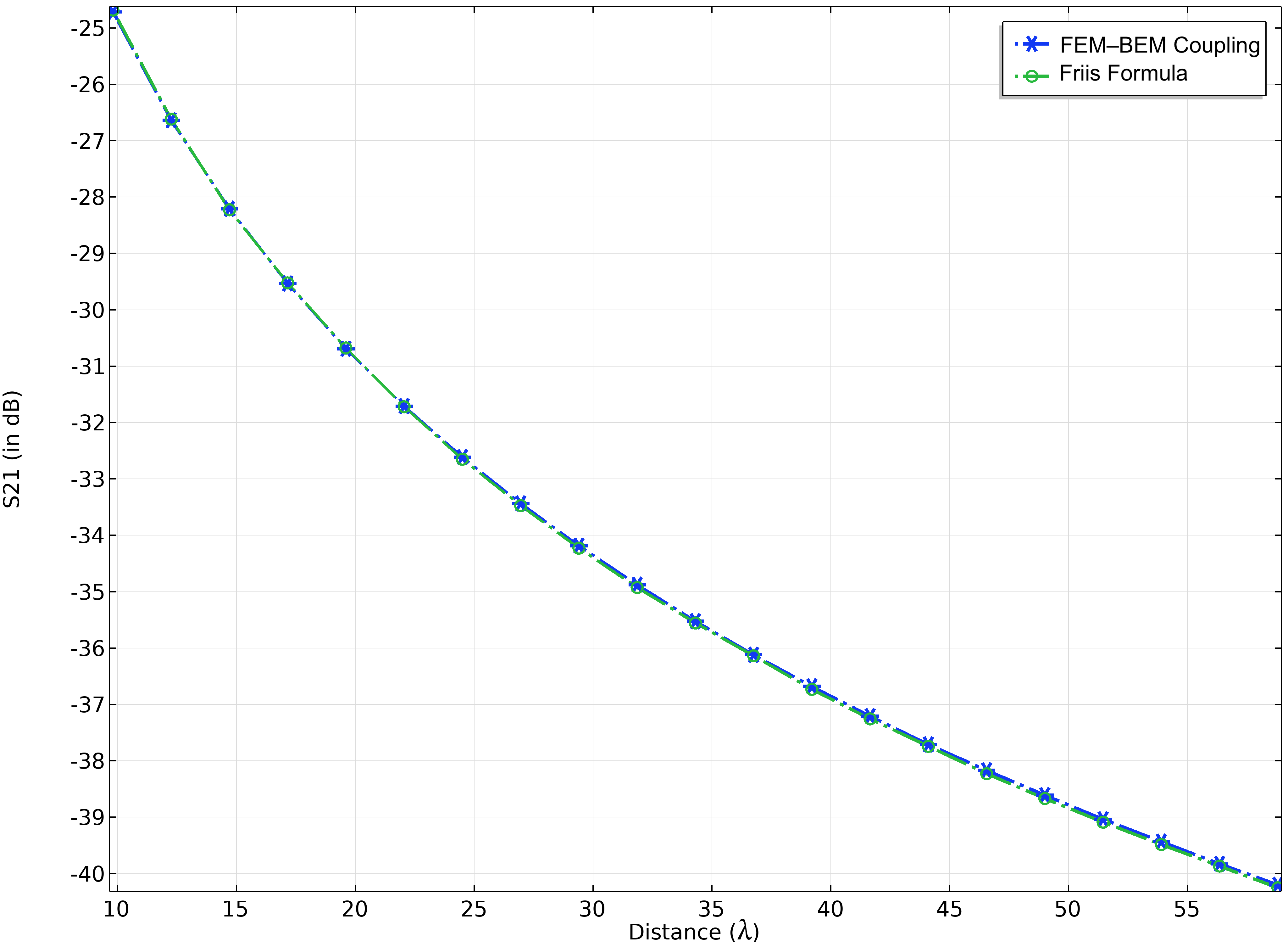
Figure 5. Comparison of the Friis formula with received power for varied distance.
Furthermore, \text {P}_\text{r} can be increased by aligning the main lobes of the antenna radiation pattern. Let’s verify this by rotating the receiver antenna at an azimuth angle. This angle variation could be from -90° to 90°. In other words, we are mimicking the antenna gain measurement setup. From Figure 6 it can be seen that the power received reaches its maximum at 0°. This configuration corresponds to both antennas having maximum gain along the x-axis.
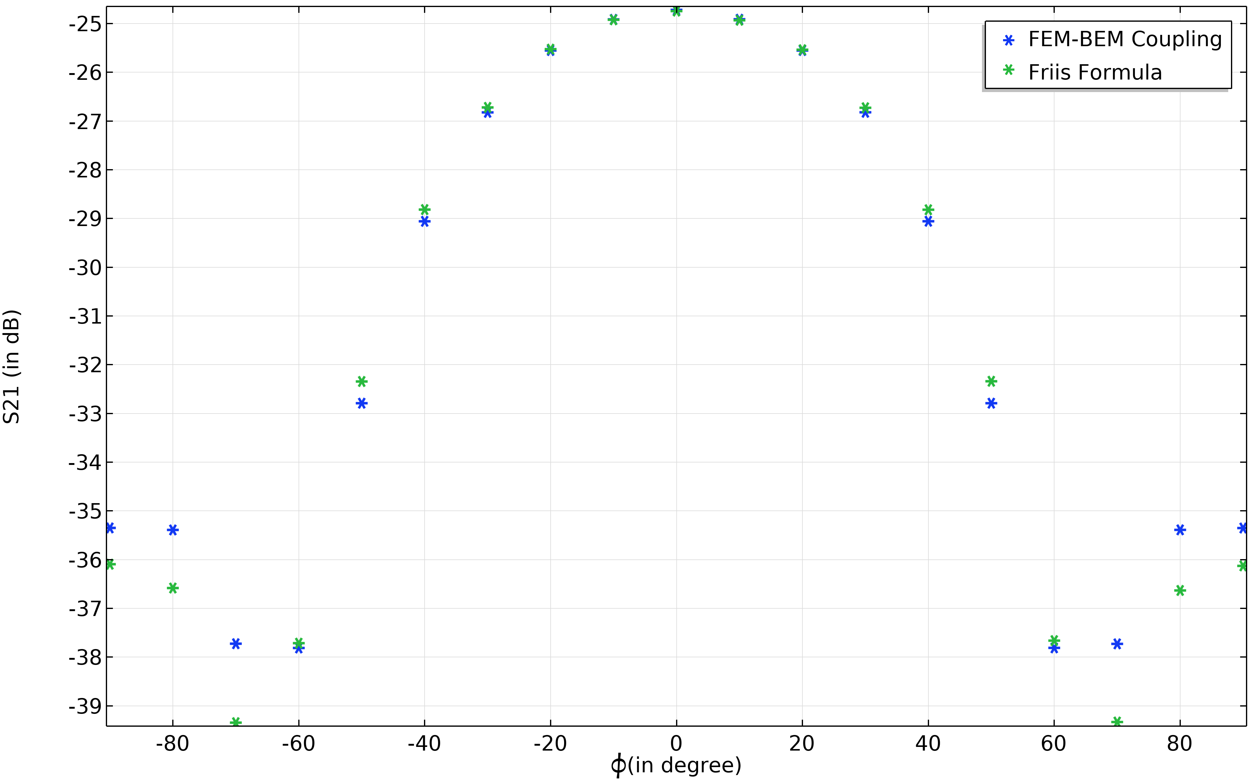
Figure 6. Comparison of the Friis formula with received power for a varied angle.
Opening Doors for EMI/EMC Testing
The beam envelope method available with the Wave Optics Module overcomes the barrier of wavelength-comparable geometry size in nonscattering EM problems, and it’s well suited for guided media. However, it is also possible to use a FEM–BEM coupling for modeling scattering EM problems without having to handle meshing requirements or geometry size restriction. One such application can be to set up an EMI/EMC test bench. For example, to perform the emission test for the RE102 military standard (up to 18 GHz frequency), the distance between the device under test (DUT) and the antenna is 1 meter. For 18 GHz of signal, a 1-meter distance is in order of 60 times wavelength, and modeling such a vast space through FEM is computationally very expensive. Instead of modeling the DUT and antenna in single FEM, we can segregate them into two FEM domains (with, of course, comparable wavelength size) and couple them with BEM, as illustrated in Figure 7. The detected power at the antenna can be a measure of radiated EM signal strength from the DUT.

Figure 7. An illustration of an EMI/EMC test bench setup for performing emission analysis.
Concluding Thoughts
FEM–BEM coupling has opened doors for extensive EM simulations, which were restricted due to meshing requirements and computational resource limitations. Verifying the Friis transmission equation makes it more reliable in simulation cases where users are interested in emission and immunity testing in EMI/EMC analysis for their DUTs.
Next Steps
Try the Verifying Friis Transmission Equation with FEM–BEM Coupling tutorial model yourself by clicking the button below, which will take you to the Application Gallery:
(Tip: Want extra modeling practice? Check out our FEM–BEM Coupling of a Microstrip Patch Antenna tutorial model.)

Comments (0)