RF Module Updates
For users of the RF Module, COMSOL Multiphysics® version 5.3 brings a Part Library for common RF devices, extended options for the Lumped Element boundary condition, and S-parameter calculation for transient simulations. Browse all of the RF Module updates in more detail below.
New RF Part Library
The RF Module has now introduced a Part Library consisting of a number of standard parts or geometries that assist in modeling RF components that can be included in larger designs of RF devices. Each part has user-controllable parameters and predefined selections that can be manipulated to change geometric configurations, RF device designs, geometry-dependent material properties, and solver settings.
The RF parts include:
- 36 rectangular waveguides (consisting of straight and 90-degree bend types as well as H-bend types)
- 22 surface-mount device footprints
- 3 SMA connectors (4 holes, 2 holes, and vertical mount)
 Two SMA connectors (4 holes and vertical mount) that are connected through a 50-Ohm meander microstrip line.
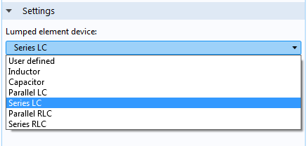
Enhanced Lumped Element Feature with Extended Options
The Lumped Element boundary condition has been improved with extra options for the Lumped element device section of its Settings window. Not only can you configure the single-lumped elements — inductor (L), capacitor (C), resistor (R), or complex impedance (Z) — as device boundary conditions, but also composite elements that involve lumped element parameters, such as series LC, parallel LC, series RLC, or parallel RLC lumped elements.
Application Library path for an example using the new lumped element options:
RF_Module/Filters/lumped_element_filter
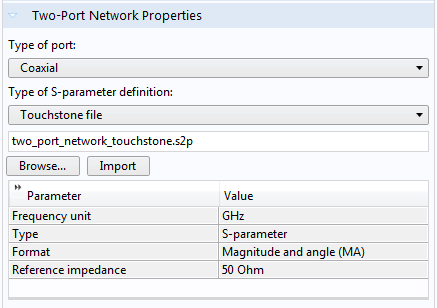
Advanced Two-Port Network Modeling with Touchstone File Import
A Touchstone file describes the frequency responses of an n-port network circuit in terms of S-parameters. A Touchstone file, obtained from numerical simulations or network analyzer measurements, can be included in COMSOL Multiphysics® simulations via the Two-Port Network boundary condition without building the complicated shape of the circuit. To do this, select Touchstone file as the Type of S-parameter definition in the Two-Port Network Settings window.
Application Library path for an example using the Touchstone file import feature:
RF_Module/Filters/two_port_network_touchstone
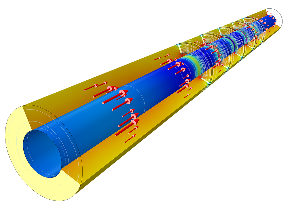
Surface Magnetic Current Density
The new Surface Magnetic Current Density boundary condition has been added to the Electromagnetic Waves, Frequency Domain interface and specifies a surface magnetic current density at both exterior and interior boundaries. Magnetic current density is described by a 3D vector. However, because it flows along a surface, it can be alternatively represented for more efficient modeling. To achieve this, the COMSOL Multiphysics® software projects this current density onto a boundary surface and neglects its normal component. The new boundary condition has been provided for special modeling situations, such as for modeling electric dipoles.

Surface magnetic current density (blue arrows) on a cylindrical coil through use of the Surface Magnetic Current Density boundary condition in the Electromagnetic Waves, Frequency Domain interface. The electric field pattern (cone) resembles that of a short dipole antenna.
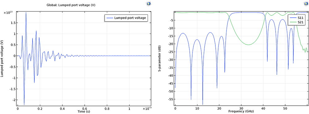
Calculate S-Parameters from Transient Simulations
Frequency-domain S-parameters of a circuit can now be calculated from time-dependent simulations by using a two-step solving process. Good for calculating wide-band frequency responses with a fine frequency resolution, models are first built using a transient physics interface. Then, the S-parameters are calculated using a time-to-frequency fast Fourier transform (FFT) on the results.
To do this, you include a Time Dependent study step using a lumped port in the Electromagnetic Waves, Transient interface, and then include a Time to Frequency FFT study step to perform the transform of the results from the first study step.
Application Library path for an example calculating S-parameters from transient simulations using a time-to-frequency FFT:
RF_Module/Filters/coaxial_low_pass_filter_transient
Updated Tutorial Model: A Low-Pass Filter Using Lumped Elements
Passive devices can be designed using lumped element features if both the operating frequency of the device and the insertion loss of lumped elements are low. This example simulates two types of lumped element filters that are similar to lumped ports, except that they are strictly passive and there are predefined choices for inductances and capacitance.
First, a five-element maximally flat low-pass filter is built to compute frequency responses that show the cutoff at the intended frequency. The geometry of each element (surface-mount device, SMD) is simplified as a 2D boundary and the electrical performance is modeled using the Lumped Element boundary condition in the Electromagnetic Waves, Frequency Domain interface. Then, a band-pass filter transformed from the low-pass filter design is simulated in the same frequency range. Both filter models present the S-parameters and electric field distribution.
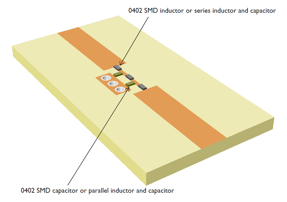 The 0402 surface-mount device (SMD) inductors and capacitors are modeled using lumped element features on 2D boundaries.
Application Library path for the low-pass filter using lumped elements tutorial model:
RF_Module/Filters/lumped_element_filter
New Tutorial Model: Anechoic Chamber Absorbing Electromagnetic Waves
An anechoic chamber is used to measure antenna characterization, electromagnetic interference (EMI), and electromagnetic compatibility (EMC). Within the chamber are absorbers that are configured with an array of pyramidal objects that steer the propagating incident field onto their neighboring absorbers. By absorbing electromagnetic waves inside the chamber and blocking incoming signals from outside, the chamber creates a virtual infinite space that has almost no internal reflections and does not suffer from any unwanted external RF noises.
This model simulates a biconical antenna, popularly used in EMI and EMC tests, which is located at the center of a small anechoic chamber. The computed far-field radiation pattern and S-parameter (S11) demonstrate that the microwave absorbers reduce reflection from the walls significantly without distorting antenna performance.
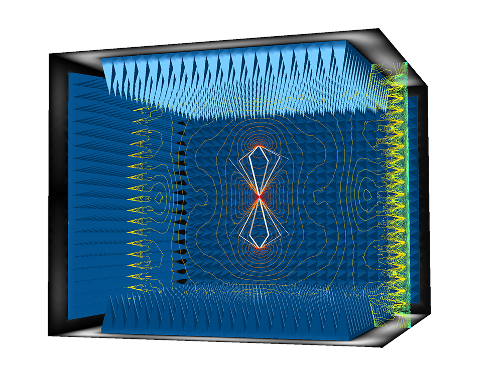
A state-of-the-art anechoic chamber, built in a small room (3.9x3.9x3.3 m), consisting of microwave absorbers on thin conductive walls. The contour plot shows the electric field distribution on the ZX-plane. This is noticeably decayed in the vicinity of the absorbers.
Application Gallery link for the anechoic chamber tutorial model:
RF_Module/EMI_EMC_Applications/anechoic_chamber
New Tutorial Model: Double-Ridged Horn Antenna
A double-ridged horn antenna is popularly used in anechoic chambers to characterize an antenna under test (AUT), from S-band to Ku-band, due to its reliable performance in a wideband frequency range. This tutorial models a double-ridged horn antenna and computes the voltage standing wave ratio (VSWR), far-field radiation pattern, and antenna directivity.
A lumped port is assigned on the boundary between the inner and outer conducting surface at the end of the coaxial connector. The outermost layer of the air domain is configured to be a perfectly matched layer (PML), which simulates the absorption of all outgoing radiation from the antenna as would occur in a real anechoic chamber. The mesh is dynamically controlled by the Electromagnetic Waves, Frequency Domain interface based on each simulation frequency.
 Double-ridged horn antenna excited by a coaxial port. This image shows the 3D far-field radiation pattern (Heat color plot), the direction of electric field (Arrow plot), and its intensity (Rainbow color plot) on the aperture and ridges.
Application Library path for the double-ridged horn antenna tutorial model:
RF_Module/Antennas/double_ridged_horn_antenna
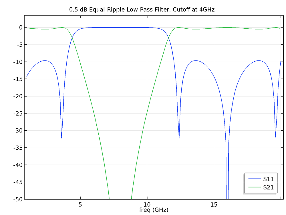
New Tutorial Model: Fast Modeling of a Transmission Line Low-Pass Filter
One way to design a filter is to use the element values of well-known filter prototypes, such as maximally flat or equal-ripple low-pass filters. It is easier to fabricate a distributed element filter on a microwave substrate than a lumped element filter, since it is cumbersome to find off-the-shelf capacitors and inductors that are exactly matched to the frequency-scaled element values of the filter prototype.
This tutorial model demonstrates the design process of a distributed element filter using Richard’s transformation, Kuroda’s identity, and the Transmission Line interface. This approach is very fast compared to solving Maxwell’s equations in 3D. The model simulates a three-element 0.5 dB equal-ripple low-pass filter that has a cutoff frequency at 4 GHz. The resulting S-parameter plot shows a low-pass frequency response that is also periodically observed at a higher frequency range.
Application Library path for the Fast Modeling of a Transmission Line Low-Pass Filter tutorial model:
RF_Module/Filters/transmission_line_lpf
New Tutorial Model: Fast Modeling of a Transmission Line Wilkinson Power Divider
Some conventional three-port power dividers are resistive power dividers and T-junction power dividers. Such dividers are either lossy or not matched to the system reference impedance at all ports. In addition, isolation between two coupled ports is not guaranteed. The Wilkinson power divider outperforms the lossless T-junction divider and the resistive divider and it does not have the previously mentioned issues.
This example model simulates a Wilkinson power divider using the Transmission Line interface in 2D. This approach is very fast compared to solving Maxwell’s equations in 3D. The results present the S-parameters from 1 GHz to 5 GHz and electric potential distribution along the transmission line.
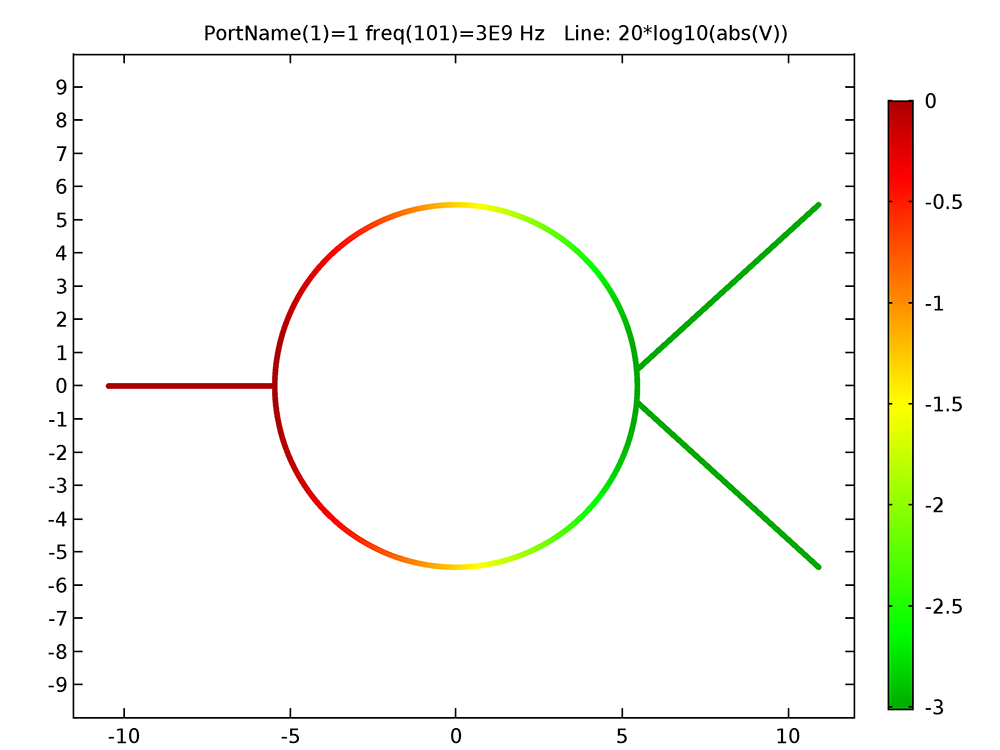 The input voltage is distributed (-3 dB) equally between port 2 and port 3 when port 1 is excited.
Application Library path for the Wilkinson power divider tutorial model:
RF_Module/Couplers_and_Power_Dividers/transmission_line_wpd
New Tutorial Model: Fast Prototyping of a Butler Matrix Beamforming Network
A Butler matrix is a passive beamforming feed network. It is a cost-effective feed network for phased array antennas because the circuit can be fabricated in the form of microstrip lines and is a viable solution for performing beam scanning without deploying expensive active devices.
This example shows how to design such a circuit using the Transmission Line interface. The results show the logarithmic voltage on the Butler matrix beamforming circuit at 30 GHz and the arithmetic phase progression at each output port.
| Port 5 | Port 6 | Port 7 | Port 8 | Phase Progression | |
|---|---|---|---|---|---|
Port 1 excited |
-90° | -135° | -180° | 135° | -45° |
Port 2 excited |
-180° | -45° | 90° | -135° | +135° |
Port 2 excited |
-135° | 90° | -45° | -180° | -135° |
Port 4 excited |
135° | -180° | -135° | -90° | +45° |
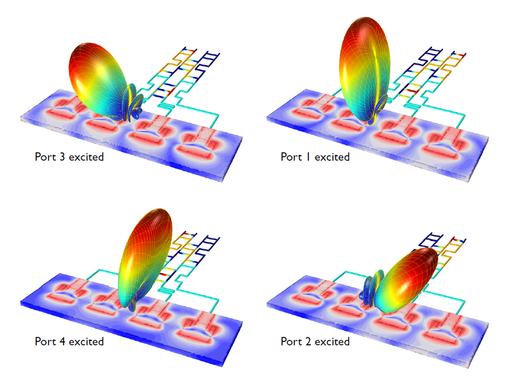 The 3D far-field radiation pattern of a 4x1 microstrip patch antenna array connected to the Butler matrix beamforming network. The images here are ordered by phase progression (negative to positive). The antenna model is not included in this example.
Application Library path for the Butler matrix beamforming network tutorial model:
RF_Module/Couplers_and_Power_Dividers/transmission_line_butler
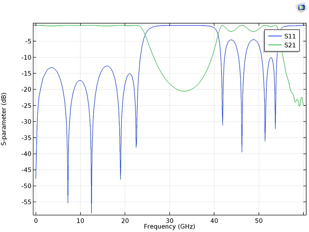
New Tutorial Model: Time-to-Frequency Fast Fourier Transform of a Coaxial Low-Pass Filter
To achieve a low-pass frequency response, an air-filled coaxial cable is tuned with five annular rings (irises) that are added to the outer conductor wall in this example model. It simulates a 2D axisymmetric, relatively wideband coaxial low-pass filter. To address the wideband frequency response with a fine frequency resolution, the model is first built with a transient physics interface, then S-parameters are calculated using a time-to-frequency FFT. The computed S-parameters show a low-pass frequency response with a cutoff frequency around 24.5 GHz.
 The contour plot of the electric field norm distribution and the arrow plot of time-averaged power flow at 10 GHz.
Application Library path for the FFT of a coaxial low-pass filter tutorial model:
RF_Module/Filters/coaxial_low_pass_filter_transient
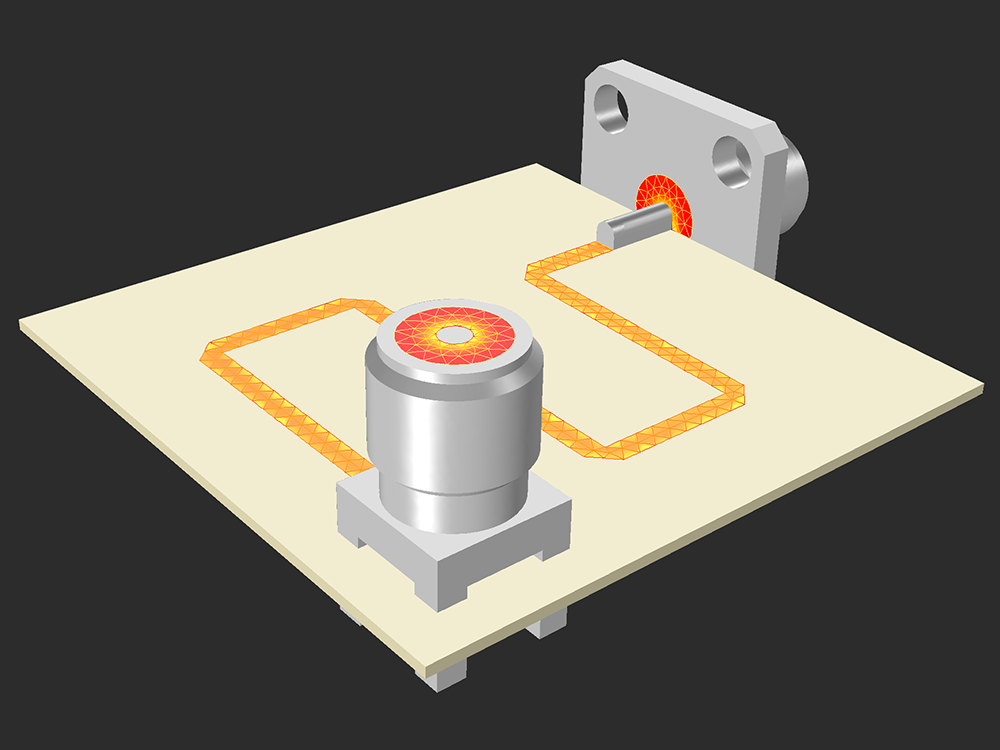
New Tutorial Model: Filter Characterized by Imported S-Parameters via a Touchstone File
A Touchstone file describes the frequency responses of an n-port network circuit in terms of S-parameters. This can be used to simplify arbitrarily complex circuits. The Touchstone file can be obtained from numerical simulations or network analyzer measurements. The obtained file for a two-port network can then be included in simulations without building the complicated shape of the circuit.
In this example, a low-pass filter between two coaxial connectors is modeled using a two-port network feature and imported S-parameters via a Touchstone file. The results include electric field distribution within the coaxial connectors and the S-parameters.
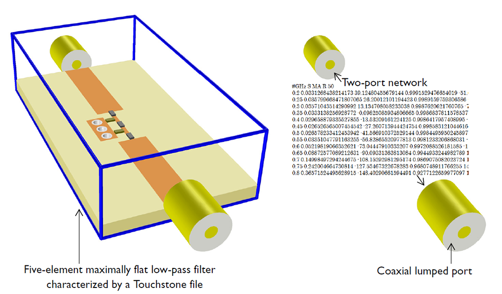 The circuit geometry inside the blue box frame is not included in the model, but characterized by a Touchstone file.
Application Library path for the S-parameter via Touchstone file import tutorial model:
RF_Module/Filters/two_port_network_touchstone
New Tutorial Model: High-Speed Interconnect Tuning by Time-Domain Reflectometry
In signal integrity (SI) applications, time-domain reflectometry (TDR) is a useful technique to analyze the discontinuity in a signal path by observing the reflected signal strength. The reflected signal distorts the input pulse mainly by impedance mismatch if there is no external noise source, crosstalk, or undesired coupling.
In this example, a staircase step function with a fast rise time is launched on a microstrip line connected from layer to layer through a metalized via hole. The signal path discontinuities are identified, and the circuit is tuned to lower the distortion based on the TDR impedance calculation.
 A microstrip line on a multilayer circuit board where a 20-mil microwave substrate is used for each dielectric layer. The ground plane with an antivia pad is located between two dielectric layers. The top and bottom microstrip lines are connected with a metalized via hole. The top dielectric surface and ground plane are removed to provide a better view.
Application Library path for the time-domain reflectometry tutorial model:
RF_Module/EMI_EMC_Applications/high_speed_interconnect_tdr
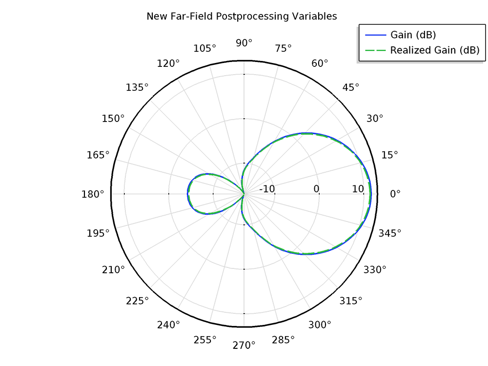
New Far-Field Postprocessing Variables
Additional postprocessing variables have been added to the physics interfaces that calculate far-field radiation patterns. The previous gain variable is clarified with gain and realized gain by the input impedance mismatching factor. These postprocessing variables can be used in far-field plots to visualize the characteristics of an antenna.
- EIRP and EIRPdB: effective isotropic radiated power and its dB-scaled value
- gainEfar and gaindBEfar: gain excluding input mismatch and its dB-scaled value
- rGainEfar and rGaindBEfar: realized gain including input mismatch and its dB-scaled value
Application Library path for the new far-field postprocessing variable:
RF_Module/Antennas/double_ridged_horn_antenna
New Default Settings for Enhanced Usability
Many default settings have been updated to reduce the number of modeling steps and enhance usability:
- Enabled physics-controlled mesh for the Electromagnetic Wave, Frequency Domain interface
- Mesh reads the frequency or wavelength from study steps automatically for the Electromagnetic Wave, Frequency Domain interface
- Solver settings changed from Robust to Fast for the Electromagnetic Wave, Frequency Domain interface
- Finer angular resolution (theta 45, phi 45) for the 3D far-field plot
- Automatic excitation is now turned on for the first port
- GHz is now the new default frequency unit for the Frequency Domain, Frequency-Domain Modal, and Eigenfrequency study steps
- Eigenfrequency search method around shift is now set to Larger real part for Frequency-Domain Modal analyses
- The Linper operator is applied internally for excited lumped ports and no longer needs to be specified by the user for Frequency-Domain Modal analyses
- GHz is now the default unit for S-parameter plots, along with simpler S-parameter descriptions
Updated Tutorial Models That Use Reduced-Order Modeling Techniques
The use of the Frequency-Domain Modal study step has been extended to lumped ports and ports without requiring a manual input of the linper operator on the excitation port voltage. Two powerful simulation methods, the asymptotic waveform evaluation and frequency-domain modal methods, have been implemented in existing Application Library examples for designing bandpass-filter-type high-Q devices. These methods solve simulations at speeds that are orders of magnitude faster with a much finer frequency resolution than conventional frequency sweeping for these devices.
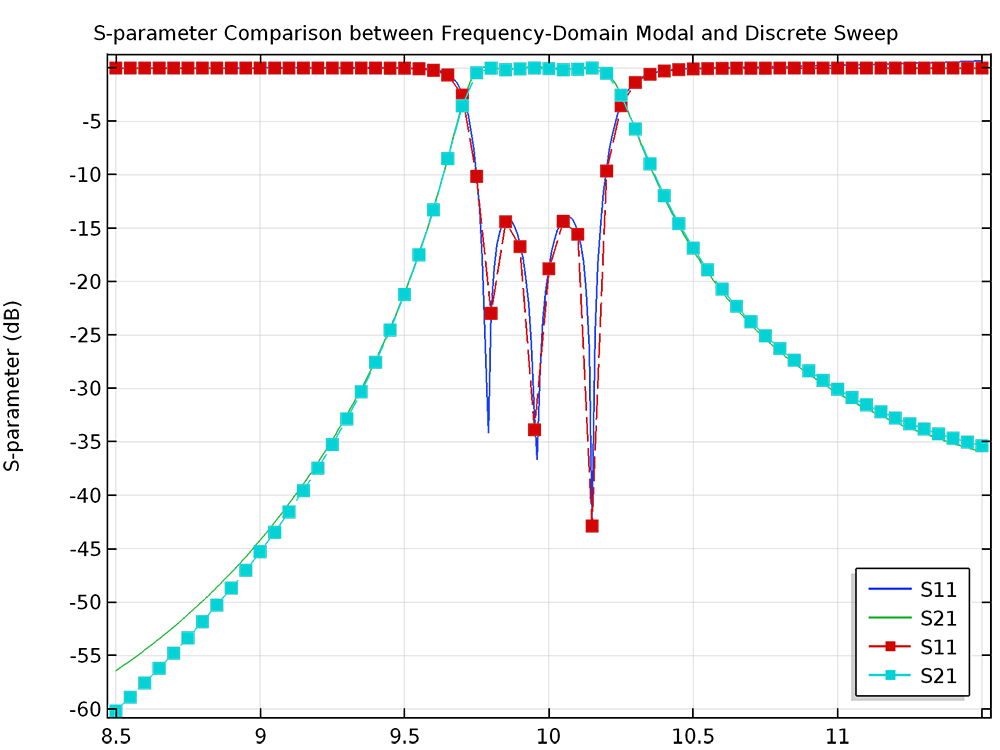
While the frequency resolution of the Frequency-Domain Modal is five times finer than that of the discrete frequency sweep, the simulation time is four times faster to analyze the same filter. This image is from the Waveguide Iris Bandpass Filter tutorial model.
Application Library paths for the examples using the Asymptotic Waveform Evaluation method:
RF_Module/Filters/cylindrical_cavity_filter_evanescent
RF_Module/Passive_devices/rf_coil
Application Library paths for the examples using the Frequency-Domain Modal method:
RF_Module/Filters/cascaded_cavity_filter
RF_Module/Filters/coupled_line_filter
RF_Module/Filters/cpw_bandpass_filter
RF_Module/Filters/waveguide_iris_filter