Multiphysics Modeling of Piezotronic Effect of ZnO Nanowires Under Arbitrary Loading
In order to exploit the piezotronic effect of Zinc Oxide (ZnO) crystal and to design an optimal high gauge strain sensors. One would require a deep understanding of the dynamics of charge carrier transport and accurately predict the levels of mechanical stress field and electrical charge-voltage inside the device. Because the diffusion current depends exponentially on the Schottky barrier height, the relationship between strain and current flow is nonlinear. Therefore, the numerical model aims at investigating and rationalizing the critical parameters that control the sensitivity, linearity and noise figure of ZnO based piezotronic sensor.
To account for the physics phenomena and key design parameters, we used COMSOL Multiphysics® software to model the piezoelectric effect of semiconductor (n-doped ZnO) and the Schottky barrier junction at the Platinum (Pt) contacts. Two COMSOL Multiphysics® Modules are required to cover all governing equations of the physics; MEMS Module which deals with the piezoelectric effect by coupling the underlay solvers Solid Mechanics (solid) and Electrostatics (es) interfaces, and the Semiconductor Module which accounts for semiconductor doping models to simulate the charge carriers dynamics.
Despite the fact that the software application libraries provide some typical modeling examples of piezoelectric or semiconductor models, however, we did not come across tutorial models that combine both Modules MEMS and Semiconductor. Here we will present an intuitive modeling solution where we cross communicate the piezo-charges and potential between the electrostatic (es) solver of MEMS Module and the electrostatic solver of the Semiconductor Module.
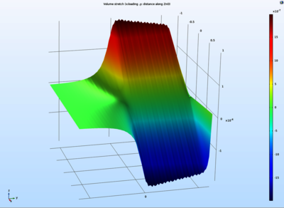
We will present the numerical model that has been set up in COMSOL Multiphysics® to study the I(V) characteristic of doped ZnO shown in Figure 1. The Nanowire has a length of 4 μm and a radius of 150 nm, the doping concentration is 1017 cm−3. It is evident that the model predicts correctly the physical behavior of piezotronic effect. When a negative strain is applied with respect to the c-axis of ZnO NW, the negative piezoelectric charges move to the top contact with platinum, while positive piezoelectric charges appear at the other contact. The free electron population moves then from the top to the bottom contact, widening the depletion region at the top junction while reducing it at the bottom one. This will induce an asymmetric barrier height at the Schottky contacts. Under a positive strain, the behavior is reversed due to symmetry. When we apply a bias voltage, the effect on charge carrier population is magnified by the presence of the piezoelectric charges due to the strain.