
Intel Optimizes an Electronic Device Component with Simulation
Juan C. Cervantes-Gonzalez, Intel Guadalajara Design Center, Mexico
As the demand grows for faster electronic devices in smaller packages, we need to develop optimized high-speed interconnects, which transfer the signal between components in electronic devices. Found in printed circuit boards (PCB), this integral design element in electronics packaging carries signals laterally and through the depth of PCBs, traversing many layers of metal and dielectric material. To satisfy these growing technology demands, interconnects must be designed smaller, more closely packed, and able to operate at higher frequencies.
To reduce the number of prototypes required to test new interconnect designs, engineers at the Intel Guadalajara Design Center developed an efficient computational design optimization method, combining full-wave electromagnetic simulation in COMSOL Multiphysics® software with a space-mapping (SM) algorithm implemented in MATLAB® software. Through their approach, an interconnect design can be quickly optimized, streamlining the design cycle and time to market of the latest high-speed interconnect technology.
Suggested Stories
Simulating Printhead Unimorph Actuators at FUJIFILM Dimatix
FUJIFILM Dimatix, a top producer of commercial inkjet printheads, uses multiphysics simulation to develop MEMS ...
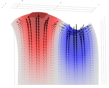
Gaining Insight into Piezoelectric Materials for Acoustic Streaming
Many sensors, such as flow sensors and those used in medical diagnostics, rely on microfluidic devices. However, ...
Illuminating Complex Material Behavior with Multiphysics Simulation
At Canadian Nuclear Laboratories, multiphysics simulation is used to gain insight into the behavior of nuclear fuel ...
Researching a New Fuel for the HFIR: Advancements at ORNL Require Multiphysics Simulation to Support Safety and Reliability
In response to the increasing awareness of the risks associated with the proliferation of nuclear materials, the ...


