
Besi Improved Memory Chip Manufacturing with Multiphysics Simulation
Stefan Behler, Besi, Switzerland
As memory chips become smaller and smaller, designers must ensure that the chips stay intact during the manufacturing process. Besi develops equipment and assembly processes for substrate and wafer packaging production in markets such as consumer electronics, automotive, industrial, and solar energy. Stefan Behler, a senior expert process engineer, used multiphysics simulation to explore and optimize a new way of peeling off the tape on a memory chip that results in less deformation of the dies. This new method is now used by semiconductor packaging factories all over the world.
Suggested Stories

Détecter la corrosion dans les conduites encastrées à l'aide de la simulation
Une nouvelle approche utilise des ondes guidées générées par la technologie EMAT afin de détecter la corrosion dans ...
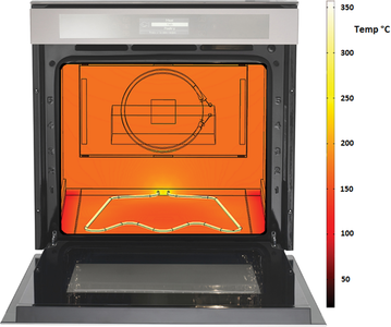
Simulation Turns Up the Heat and Energy Efficiency at Whirlpool Corporation
Engineers working on a joint research project between Whirlpool Corporation and the European initiative GREENKITCHEN ...
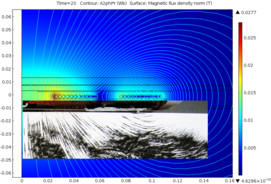
Multiphysics Simulation Helps Miele to Optimize Induction Stove Designs
The induction stove was designed to meet a consumer need for better precision and speed than traditional stoves. ...
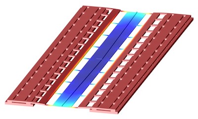
Designing a Silicon Photonic MEMS Phase Shifter with Simulation
Researchers at the Swiss Federal Institute of Technology Lausanne are using simulation to optimize the optical and ...


