
Besi Improved Memory Chip Manufacturing with Multiphysics Simulation
Stefan Behler, Besi, Switzerland
As memory chips become smaller and smaller, designers must ensure that the chips stay intact during the manufacturing process. Besi develops equipment and assembly processes for substrate and wafer packaging production in markets such as consumer electronics, automotive, industrial, and solar energy. Stefan Behler, a senior expert process engineer, used multiphysics simulation to explore and optimize a new way of peeling off the tape on a memory chip that results in less deformation of the dies. This new method is now used by semiconductor packaging factories all over the world.
Suggested Stories
Multiphysics Simulations Help Track Underground Fluid Movements
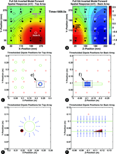
Combining acoustic and electromagnetic analyses helps scientists to more efficiently measure and survey subterranean ...
Keeping Cool: SRON Develops Thermal Calibration System for Deep-Space Telescope
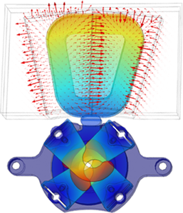
Deep-space telescopes require ultrasensitive detectors and calibration to pick up weak far-infrared signals. The SpicA ...
When it’s Impossible to Take Actual Measurements, Multiphysics Provides the Answers
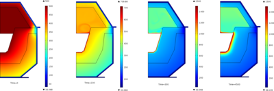
To contain splashes and provide protection at plants where metal is fabricated, blast furnace runners need a roof made ...
Reduced-Weight Reaction Sphere Makes Way for Extra Satellite Payload
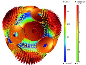
CSEM is a private applied research and development center specializing in micro-technology, system engineering, micro ...


