FSI Analysis of Wafer-to-Wafer (W2W) Direct Bonding Process
Application ID: 151871
In direct bonding, the in-plane relative displacement between corresponding points on the bonding surfaces of the top and bottom wafers, denoted as IPD (In-Plane Distortion), is the primary yield killer in the bonding process. This model can predict the entire direct wafer bonding process: wafer flattening, downward pressing contact, bonding wave propagation, and load removal. Ultimately, it provides the W2W bonding wave velocity, IPD, warpage, and stress distribution under different process parameters.
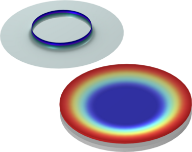
This model example illustrates applications of this type that would nominally be built using the following products:
however, additional products may be required to completely define and model it. Furthermore, this example may also be defined and modeled using components from the following product combinations:
The combination of COMSOL® products required to model your application depends on several factors and may include boundary conditions, material properties, physics interfaces, and part libraries. Particular functionality may be common to several products. To determine the right combination of products for your modeling needs, review the Grille des spécifications and make use of a free evaluation license. The COMSOL Sales and Support teams are available for answering any questions you may have regarding this.