- Bridging the Terahertz Gap
- Modeling the Lithium-Ion Battery
- Protection contre la Corrosion
- Modélisation des batteries
- Modélisation et Simulation dans le développement des piles à combustible
- Modélisation thermique des petits satellites
- Analyse électro-vibroacoustique d'un transducteur à armature équilibrée
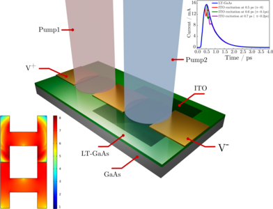
Epsilon-Near-Zero ITO Bolometer Gated by LT-GaAs: A COMSOL Study
1.Introduction Transparent conductive oxides (TCOs) operating near their epsilon-near-zero (ENZ) point have recently been shown to exhibit strong and ultrafast intraband optical absorption processes, whose excitation results in a variation of the effective mass and electrical conductance of the film [1,2]. Combined with their CMOS-compatibility, tunablity, and broadband operation, TCOs near ENZ represent a potential avenue for integrated bolometeric detectors [3]. In this work, we study a hybrid bolometer that combines a photoconductive LT-GaAs section with an ENZ film comprising indium thin oxide (ITO), to generate picosecond, delay-controlled current waveforms for photonic integrated circuits. When the ITO is excited by a laser near its ENZ condition, the absorbed light energy is transferred to the electrons, increasing their electron temperature. Hotter electrons occupy higher energy states in the conduction band, which correspond to a larger effective mass. This reduces mobility and raises resistance, providing a fast, optically controlled gate for the bolometer response [4].
2.Device structure The presented device consists of a 3 µm LT-GaAs layer on a GaAs substrate, followed in series by a thin ITO section contacted with gold trace electrodes. A central float pad connects the LT-GaAs-generated current pulse into the ITO region. A 775 nm pump excites the LT-GaAs to produce an ultrafast current impulse. A second, time-delayed pump in the telecom band illuminates the ITO, whose doping level is set so that its ENZ wavelength lies near 1550 nm. Figure 1(a) shows the structure of device, including bias ports.
3.COMSOL Multiphysics® simulation A 2D transient model is employed for COMSOL Multiphysics® simulation [5]. The LT-GaAs region is analyzed using the Semiconductor Module, which includes optical generation at 775 nm as well as Shockley Read Hall (SRH) recombination with user-defined carrier lifetimes [6]. The intraband optical absorption of ITO is modeled through optically-driven changes in effective mass, affecting mobility, and through the influence of plasma frequency on permittivity, as described by the Drude model. In this model, the plasma frequency is determined by the carrier density and the effective mass. Because of the nonparabolic nature of the ITO conduction band, hot electrons lead to an increase in effective mass and a reduction in mobility [2].
4.Results Initially, we investigate the excitation of the LT-GaAs alone using a 775 nm pump laser with a 110 µm spot size, 20 GW/cm² peak intensity, and 100 fs pulse duration. In this case, the device delivers a single, clean picosecond impulse at the readout terminals due to the increase in conductivity caused by free carrier generation; the simulated curve in Figure 1(b) reports the response without ITO excitation and sets the baseline pulse width and amplitude. Following, the ITO region is excited with a 1540 nm pump pulse (100 fs duration, 110 µm spot size, 20 GW/cm² peak intensity), which is applied with a variable delay (?) relative to the LT-GaAs excitation. This photo-activated style experiment allows us gate the device in an ultrafast manner and increase our ability to observe the THz response speed of the ITO material. When the delayed pump excites the ITO near ENZ point, the increase in effective mass results in an increase in the ITO resistance causing an additional modulation to form in the output current. We model the interaction of the ITO pump and the effective mass modulation by altering m* with a prescribed waveform. In our simulations, m* varies from 0.35m0 to 0.55m0, corresponding to a peak change of 0% to ~100% modulation, with rise and fall times of 50 fs and 200 fs, respectively. These values are within the range of existing experiments and simulations, as discussed in [2]. Figure 1(b) displays waveforms for several pump delays. The dip in the current shifts in time according to the optical delay, reflecting the moment when the ITO is excited . Figure 2(a) illustrates the logarithmic electron concentration in the LT-GaAs cross section, showing carrier generation induced by laser excitation. To clarify the hybrid bolometer mechanism, Figure 2 (b) and (c) shows logaritmic electric field and current-density distributions with ITO. Near ENZ, the normal electric field in ITO is enhanced and the current density briefly diverts away from the ITO path during the mobility trough, producing the observed dip at the terminals.
5.Conclusion In Summary, we study the bolometric response of an ENZ-tuned ITO load by coupling it to a LT-GaAs photoconductive switch. The ITO layer is found to yield a picosecond response, delay-programmable gating mechanism at telecom wavelengths. The approach is broadband, compact, and compatible with standard processes, supporting on-chip sampling, pulse shaping, and fast readout in photonic integrated circuits.