Modeling Argon Ion Sputtering on a Silicon Surface
Application ID: 140971
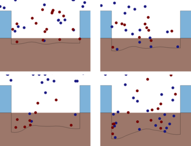
Ion beam etching is a critical technique widely used in semiconductor manufacturing, materials science, and microelectromechanical systems (MEMS). This proof-of-concept model simulates argon ion sputtering of a silicon surface using the Charged Particle Tracing interface. A Deformed Geometry interface is used to capture sputter-driven surface evolution, enabling visualization and analysis of morphology changes.
Check out our accompanying blog post on this model: “Modeling Argon Sputtering on a Silicon Surface”.
This model example illustrates applications of this type that would nominally be built using the following products:
however, additional products may be required to completely define and model it. Furthermore, this example may also be defined and modeled using components from the following product combinations:
The combination of COMSOL® products required to model your application depends on several factors and may include boundary conditions, material properties, physics interfaces, and part libraries. Particular functionality may be common to several products. To determine the right combination of products for your modeling needs, review the Grille des Spécifications and make use of a free evaluation license. The COMSOL Sales and Support teams are available for answering any questions you may have regarding this.